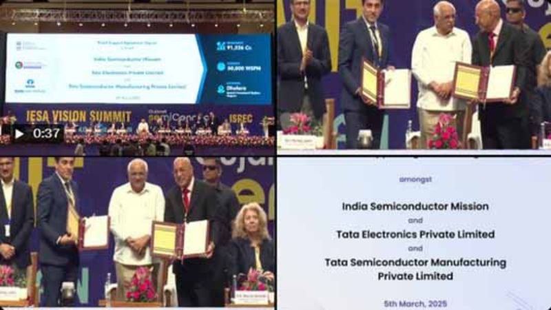
In a landmark development for India’s semiconductor industry, India Semiconductor Mission (ISM), Tata Electronics Pvt Ltd (TEPL), and Tata Semiconductor Manufacturing Pvt Ltd (TSMPL) have signed a Fiscal Support Agreement (FSA) for setting up India’s first commercial semiconductor fabrication plant (fab) in Dholera, Gujarat. The agreement was signed in the presence of Gujarat’s Chief Minister, Shri Bhupendra Patel, marking a historic step toward India’s technological self-reliance.
This strategic initiative is set to position India as a major global player in semiconductor manufacturing, strengthening the country’s technological ecosystem under the Government of India’s Modified Programme for Semiconductor and Display Manufacturing Ecosystem.
Massive Investment and Production Capacity
Contents
Tata Electronics’ semiconductor fab in Dholera Special Investment Region (SIR) will be established with a massive investment of over ₹91,000 crore (approximately $11 billion). The facility will have a production capacity of 50,000 wafer starts per month (WSPM), making it one of the largest and most advanced semiconductor plants in the region.
The Government of India, through the India Semiconductor Mission (ISM), will provide 50% fiscal support on a pari-passu basis for eligible project costs. This significant financial backing underscores India’s commitment to creating a robust, world-class semiconductor manufacturing ecosystem.
Boost to Employment and Technological Expertise
The project is expected to generate over 20,000 direct and indirect skilled jobs in India. This includes high-end technical roles, production jobs, and support functions, creating a wave of employment opportunities in the tech and manufacturing sectors.
Tata Electronics has partnered with Taiwan’s Powerchip Semiconductor Manufacturing Corp. (PSMC) to bring cutting-edge expertise and technology to India. This strategic partnership will enhance India’s capability to manufacture semiconductors for critical sectors, including:
✅ Automotive
✅ Computing
✅ Communications
✅ Artificial Intelligence (AI)
By leveraging PSMC’s technological know-how, Tata Electronics aims to establish a globally competitive semiconductor manufacturing facility, transforming India from a technology consumer to a major technology producer.
Government’s Commitment to Semiconductor Industry
Shri Sushil Pal, CEO of India Semiconductor Mission, expressed confidence in the success of the project, stating:
“The Government of India is committed to the timely disbursement of fiscal support for this project. This initiative highlights India’s ambitions in indigenous semiconductor manufacturing. Tata Electronics will play a pivotal role in strengthening the electronics value chain and contributing to India’s goals in this sector.”
This project aligns with the Government of India’s vision of technological self-reliance and positions the country as a reliable partner in the global semiconductor supply chain.
Vision of “Chips for Viksit Bharat”
Dr. Randhir Thakur, CEO and MD of Tata Electronics, called the agreement a historic milestone, saying:
“This is a historic milestone for Tata Electronics and India in establishing a semiconductor manufacturing industry. The Fiscal Support Agreement (FSA) solidifies our partnership with MeitY and ISM to realize our Hon’ble Prime Minister’s vision of manufacturing ‘Chips for Viksit Bharat.’
“We are grateful to MeitY and ISM leadership for their unwavering support and for operationalizing a globally competitive subsidy framework through this FSA. With construction underway with a strong sense of urgency, Tata Electronics is committed to building India’s first AI-enabled fab in Dholera.”
Strengthening India’s Global Position in Semiconductors
This strategic semiconductor fab will enable India to reduce its dependence on foreign semiconductor imports, ensuring greater control over critical supply chains. It will also enhance India’s position as a reliable and competitive player in the global semiconductor market.
Key benefits of the project include:
✅ Reduced reliance on imported semiconductors
✅ Strengthened technological self-sufficiency
✅ Enhanced global competitiveness in chip manufacturing
✅ Development of a skilled workforce in semiconductor manufacturing
Why Dholera is the Perfect Location
Dholera Special Investment Region (SIR) is emerging as a strategic hub for industrial and technological development. The region offers:
- Advanced infrastructure
- Proximity to major ports and transport networks
- Supportive government policies and incentives
- Availability of skilled workforce
Dholera’s infrastructure and government-backed incentives make it an ideal location for this high-tech project, reinforcing India’s growing importance in the global semiconductor landscape.
Conclusion
The establishment of Tata Electronics’ semiconductor fab in Dholera marks a defining moment in India’s technological journey. With strong financial backing from the Government of India, strategic collaboration with PSMC, and Tata’s expertise, this project will drive innovation, create employment, and position India as a global semiconductor powerhouse.
This initiative is more than just a manufacturing plant — it is a stepping stone toward India’s technological self-reliance and leadership in the global semiconductor industry.
